Fig. 1 and Fig. 2 show the transmission electron micrograph and selected area electron diffraction pattern calibration of the austenite structure in the matrix of ductile iron after austempering at 920 ℃ / 2H + 280 ℃ / 1.5h. The electron diffraction patterns of regions a, B and C in Fig. 1 (a) are shown in Fig. 1 (a), (b) and (c), respectively. Fig. 2 (a) shows the TEM photos of the interior of the needle, and Fig. 2 (b) and (c) show the local enlarged images of Fig. 2 (a). Fig. 2 (d) shows the electron diffraction pattern of Fig. 2 (c), and there are two sets of electron diffraction patterns. Fig. 2 (E) and (f) respectively show the dark field images corresponding to the two sets of electron diffraction patterns. Combining the method of crystal plane spacing and characteristic quadrilateral, and referring to the table of characteristic parallelogram of electron diffraction patterns of cubic crystal system, the electron diffraction patterns in Fig. 1 and Fig. 2 are calibrated respectively

(1) Region a consists of α – Fe and γ – Fe phases;
(2) Region B is α – Fe phase;
(3) Region C is composed of α – Fe and γ – Fe phases;
(4) The black sheet in Fig. 2 (c) is α – Fe phase;
(5) The gray and white flakes in Fig. 2 (c) are γ – Fe phase.
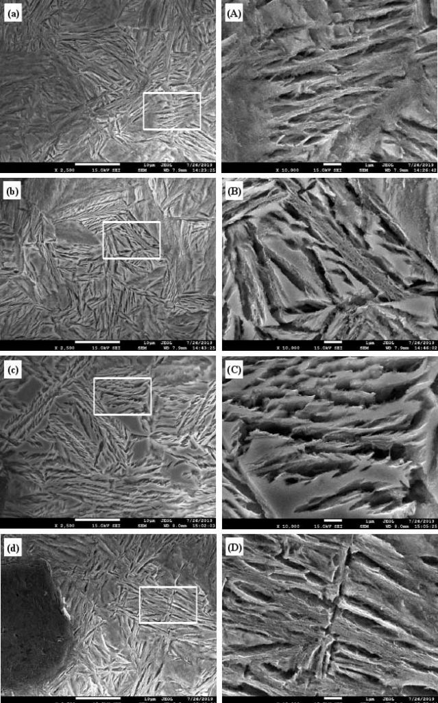
The TEM analysis of ultra fine austenite obtained by isothermal transformation at low temperature (280 ℃) shows that a cluster of ultra-fine ferrite with thickness of about 1 μ m changes from nano high carbon austenite sheet (thickness of about 36 nm ~ 57 nm) and nano ferrite sheet (thickness of about 30 ~ 57 nm) There is no carbide at the grain boundary of nano high carbon austenite sheet / nano ferrite sheet. At the same time, there are different orientations of austenite between two adjacent clusters of ultra-fine ferrite. The orientation angle is about 20 ° to 25 ° in Fig. 3 (a), (b), (c), (D), (E) and (f) of SEM.

